Thinner is better for solar cells
By EPR Magazine Editorial January 28, 2020 2:31 pm IST
By EPR Magazine Editorial January 28, 2020 2:31 pm IST

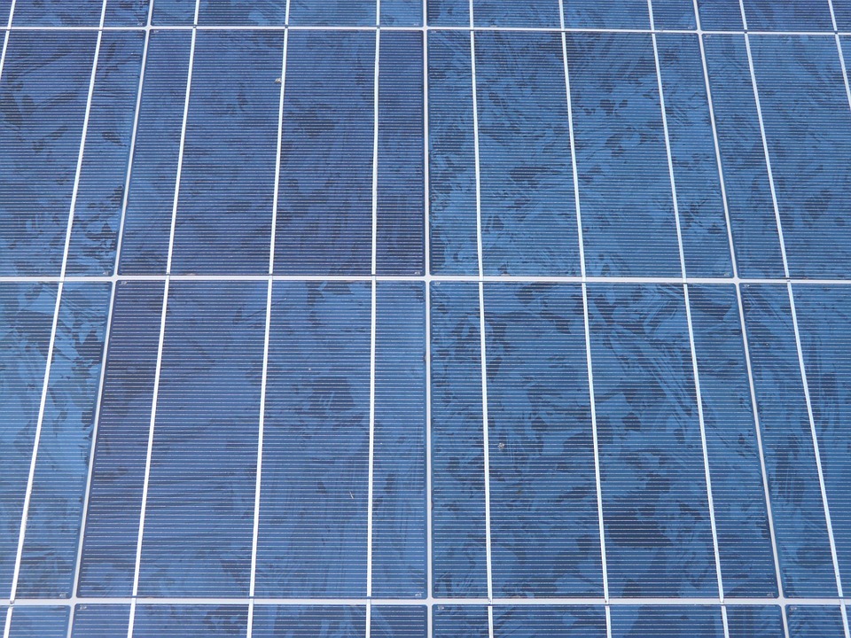
Solar panel costs have dropped lately, but slimming down silicon wafers could lead to even lower costs and faster industry expansion.
Costs of solar panels have plummeted over the last several years, leading to rates of solar installations far greater than most analysts had expected. But with most of the potential areas for cost savings already pushed to the extreme, further cost reductions are becoming more challenging to find.
Now, researchers at MIT and at the National Renewable Energy Laboratory (NREL) have outlined a pathway to slashing costs further, this time by slimming down the silicon cells themselves.
Thinner silicon cells have been explored before, especially around a dozen years ago when the cost of silicon peaked because of supply shortages. But this approach suffered from some difficulties: The thin silicon wafers were too brittle and fragile, leading to unacceptable levels of losses during the manufacturing process, and they had lower efficiency. The researchers said that there are now ways to begin addressing these challenges through the use of better handling equipment and some recent developments in solar cell architecture.
The new findings are detailed in a paper in the journal Energy and Environmental Science, co-authored by MIT postdoc Zhe Liu, professor of mechanical engineering Tonio Buonassisi, and five others at MIT and NREL.
The researchers describe their approach as “technoeconomic”, stressing that at this point economic considerations are as crucial as the technological ones in achieving further improvements in affordability of solar panels.
Currently, 90 percent of the world’s solar panels are made from crystalline silicon, and the industry continues to grow at a rate of about 30 percent per year, the researchers said. Today’s silicon photovoltaic cells — the heart of these solar panels — are made from wafers of silicon that are 160 micrometres thick. But with improved handling methods, the researchers proposed that this could be shaved down to 100 micrometres — and eventually as little as 40 micrometres or less, which would only require one-fourth as much silicon for a given size of panel.
That could not only reduce the cost of the individual panels, but even more importantly it could allow for rapid expansion of solar panel manufacturing capacity. That’s because the expansion can be constrained by limits on how fast new plants can be built to produce the silicon crystal ingots that are then sliced thin to make the wafers. These plants, which are generally separate from the solar cell manufacturing plants themselves, tend to be capital-intensive and time-consuming to build, which could lead to a bottleneck in the rate of expansion of solar panel production. Reducing wafer thickness could potentially alleviate that problem, the researchers said.
The study looked at the efficiency levels of four variations of solar cell architecture, including passivated emitter and rear contact (PERC) cells and other advanced high-efficiency technologies, comparing their outputs at different thickness levels. The team found there was in fact little decline in performance down to thicknesses as low as 40 micrometres, using today’s improved manufacturing processes.
“We see that there’s this area (of the graphs of efficiency versus thickness) where the efficiency is flat,” Liu said, “and so that’s the region where you could potentially save some money.” Because of these advances in cell architecture, he said, “We really started to see that it was time to revisit the cost benefits.”
Changing over the huge panel manufacturing plants to adapt to the thinner wafers will be a time-consuming and expensive process, but the analysis shows the benefits can far outweigh the costs, Liu said. It will take time to develop the necessary equipment and procedures to allow for the thinner material, but with existing technology, he said, “It should be relatively simple to go down to 100 micrometres,” which would already provide some significant savings. Further improvements in technology such as better detection of microcracks before they grow could help reduce thicknesses further.
Authored by:We use cookies to personalize your experience. By continuing to visit this website you agree to our Terms & Conditions, Privacy Policy and Cookie Policy.